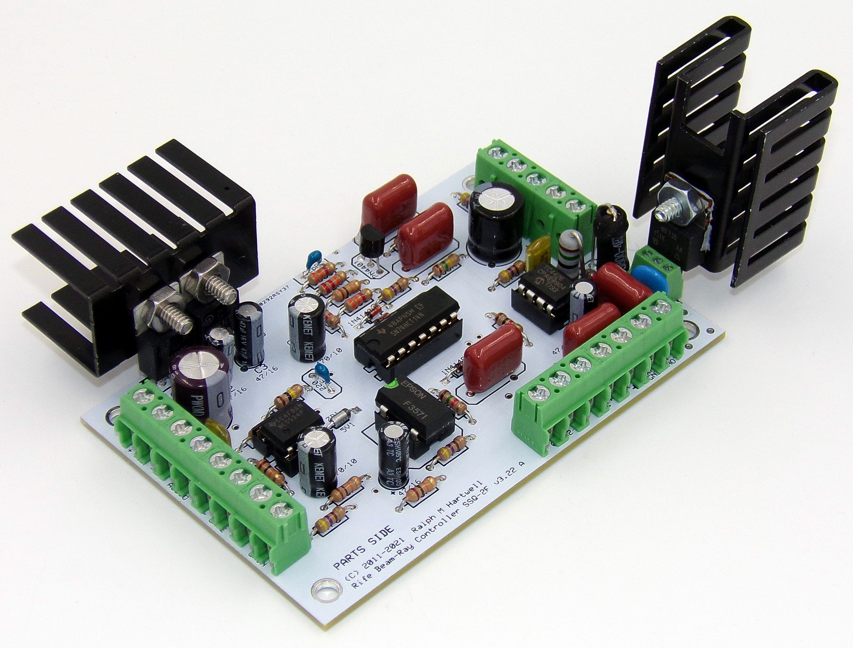
The SSQ-2F Controller Board v3.23
With all the signal processing ability of the SSQ-2F v1.41, the new SSQ-2F v3.23 also includes an input for a Gate modulation signal and an on-board medium power MOSFET RF power amplifier that can provide up to 70 watts of peak carrier power at 3.1 or 3.3 MHz.The RF output of the SSQ-2F v3.23 is sufficient to drive a high-power vacuum tube RF amplifier.
When combined with the LC31 coupler, the SSQ-2F v3.23 will drive a moderate size Rife plasma tube without the need for an external RF amplifier.
The SSQ-2F v3.23 can be supplied with your choice of either 3.1 MHz or 3.3 MHz carrier frequency oscillators.
Complete technical details and setup
information for the SSQ-2F v3.23 is available in the
Instruction Manual.
Overview -
- This SSQ-2F Rife System Controller is a control system that allows full implementation of the Jeff Garff Rife "Big Sweep" protocol using a 3.1 or 3.3 MHz carrier combined with a wide-range audio frequency sweep. For further information about this, please see: http://rifevideos.com/dr_rife_and_philip_hoylands_3.3mhz_sweep.html and http://rifevideos.com/pdf/a_history/the_rife_machine_report_a_history_of_rifes_instruments_and_frequencies.pdf
- The SSQ-2F Rife System Controller allows the use of a standard computer sound card, an MP3 player, a CD or a DVD player instead of an expensive frequency-function generator to generate the audio signal.
- A standard frequency or function generator may be used as the audio frequency source, if desired.
- Depending on the operating mode, the Rife System Controller will accept sine, square, or triangle waveform audio signals.
- A wide range of audio input levels may be used.
- The 3.1 MHz RF carrier may be square wave duty cycle modulated between 0 to 100%.
- The square wave modulation is selectable in two separate ranges; 0 to 50%, or 50 - 100%.
- The plug-in carrier oscillator module may easily be changed by the user to obtain a custom carrier frequency.
- The Controller can be set to use the modulation frequency directly, (1x Mode,) or it can be set to double the modulation frequency, (2x Mode.)
- Connections are provided for optional square wave duty cycle metering using either a user provided meter or the accessory M1D meter.
- Connections are provided for an external audio gain potentiometer using either a user provided potentiometer or the accessory R2 potentiometer.
- The level of the modulated RF output signal is adjustable from zero to 70 watts by adjusting the DC power supply voltage.
- This is a professionally manufactured etched printed circuit board with 3-ounce, tin plated, copper traces and plated-through holes. All parts are high-quality through-hole components.
- Electrolytic capacitors are rated for operation at 105 C for reliability.
- Resistors are high stability carbon or metal film, 5% tolerance.
- The active devices are socket mounted for easy, solder-free replacement if necessary.
- The SSQ-2F Controller Board is available assembled and fully tested, or as a do-it-yourself kit. A parts kit,and the printed circuit board, are also available.
- Screw terminals are provided for all connections to the Controller Board - there are no wires to solder!
- 1-year warranty against
manufacturing defects.
SPECIFICATIONS:
DC Power Supply Input:
- SSQ-2F v3.23 Logic Circuits +15 to +30 volts DC maximum,
filtered, but need not be regulated, at 0.1 Ampere, 0.25
Ampere when supplying DC power to the cooling fan on the
PA1 amplifier.
- SSQ-2F v3.23 RF amplifier +12 to
+70 volts DC filtered and regulated at 1.5 amperes
maximum, current required varies with power output and
modulation duty cycle. Nominal current less than 1.0
Ampere for 70 watts output with 50% duty cycle modulation.
Input Audio Signal Waveform:
- Sine,
triangle, or symmetrical square wave.
Modulation Modes:
- 1X Mode - The modulation
frequency equals the input audio frequency using sine,
triangle, or square waves.
- 2 X Mode - The modulation
frequency equals TWICE the input audio frequency using
sine or triangle waves only.
Carrier Frequency:
- 3.1 (standard) or 3.3 MHz.
Frequency to be specified at time of order. The carrier
frequency may be changed by the user by replacing the
plug-in oscillator module with a module of a different
frequency.
- Customer requested frequencies in
the range of 2.6 MHz to 3.8 MHz are available on special
order.
RF Power Output:
- 1) When set up for driving a
plasma tube or when used as an exciter for an external
vacuum tube RF amplifier, the SSQ-2F will produce up to
100 watts peak power, 50 watts average power as measured
across a 50-ohm load when the carrier is modulated by a
50% duty cycle square wave.
- 2) When operating as a driver for
an external solid state RF amplifier (other than the PA1,)
the SSQ-2F will produce up to 15 watts peak, 7.5 watts
average power as measured across a 50 ohm load when the
carrier is modulated by a 50% duty cycle square wave. It
is necessary to perform a slight modification to the
SSQ-2F for this use.
- 3) When operating as a driver for
a contact system, the SSQ-2F will produce up to 72 volts.
- The RF output power output from
the SSQ-2F in cases (1) and (2) and the RF output voltage
output in case (3) are adjustable by varying the DC
voltage input to the RF amplifier PA PWR terminal
block of the SSQ-2F.
Modulation Frequency Ranges - 2 X Mode:
Input Audio Frequency Range in 2 X Mode @ 40 - 3500 mV p/p input level with a Sine or Triangle Wave Input Signal:
- Low
- 40 Hz.
- High
- 30,000 Hz at maximum audio gain, or 60,000 Hz at minimum
audio gain.
- This
will square wave modulate the carrier over the range of 80
to 60,000 Hz or 80 to 120,000 Hz.
NOTE: In
the 2 X mode, using a sine or triangle wave audio input, the
output of the Controller Board will maintain a 50% duty
cycle ratio to within 10% or less across the input frequency
range of 40 to 30,000 Hz at maximum audio gain, or 40 to
60,000 Hz at minimum audio gain. This allows unattended
operation of the equipment without the need for constant
audio gain adjustments when using an audio sweep signal
generated by a computer sound card. It is necessary to
maintain a low source impedance and a constant voltage as
the audio frequency changes during the sweep.
Modulation Frequency Ranges - 1 X Mode:
Input Audio Frequency Range in 1X Mode, @ 50 - 3500 mV p/p Input Level with a Sine or Triangle Wave Input Signal:
- Low
- 6 Hz.
- High
- 200,000.
- This
will square wave modulate the carrier over the range of 4
to 200,000 Hz.
- Usable
frequency range from 4 to 400,000 Hz with increased audio
input level.
- This
will square wave modulate the carrier over the range of 4
to 400,000 Hz.
Modulation Frequency with a Square Wave input signal of 50 - 3500 mV p/p:
Note: Square wave audio is usable in 1X Mode only, and a 50% duty cycle is output by the Controller Board.
- Low
- 75 Hz.
- High
- 200,000 Hz.
- This
will square wave modulate the carrier over the range of 75
to 200,000 Hz.
- Usable
frequency range from 50 to 600,000 Hz with increased audio
input level.
- This
will square wave modulate the carrier over the range of 50
to 600,000 Hz.
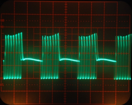
SSQ-2F Waveforms
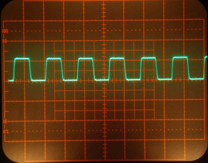
3.1 MHz RF Carrier Oscillator
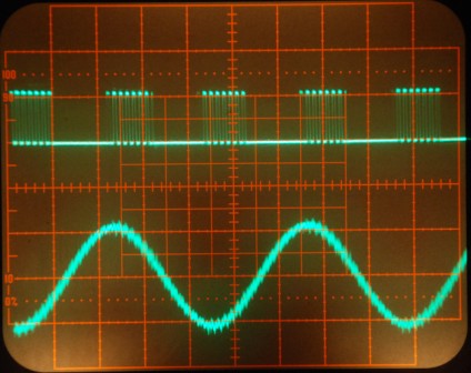
Lower Trace = 6 KHz audio sine wave input to the SSQ-2F
Upper Trace = Modulated 3.1 MHz RF Carrier output, modulated at a 6 KHz rate with a 50% duty cycle square wave. This is the non-frequency doubled mode of operation of the SSQ-2F.
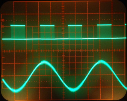
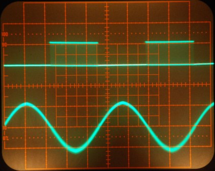
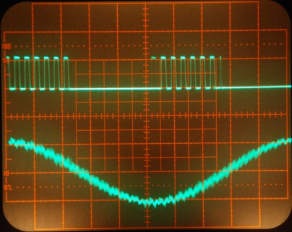
Lower Trace = 6 KHz audio sine wave input to the SSQ-2F
Upper Trace = Modulated 3.1 MHz RF Carrier output, modulated at a 12 KHz rate with a 50% duty cycle square wave. This is the frequency doubled mode of operation of the SSQ-2F.
Lower Trace = 194 KHz audio sine wave input to the SSQ-2F
Upper Trace = Modulated 3.1 MHz RF Carrier output, modulated at a 388 KHz rate with a 50% duty cycle square wave. This is the frequency doubled mode of operation of the SSQ-2F. Note that individual cycles of the 3.1 MHz carrier may be seen in the upper trace. Also note the very short rising and falling edges of the modulated 3.1 MHz RF carrier signal.
Same as the above picture, but zoomed in to show the very fast edges of the modulated 3.1 MHz RF carrier signal.
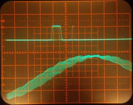
Lower Trace = 155 KHz audio sine wave input to the SSQ-2F
Upper Trace = Modulated 3.1 MHz RF Carrier output, modulated at a 310 KHz rate with a 10% duty cycle square wave. This is the frequency doubled mode of operation of the SSQ-2F. Note that there is only one cycle of the 3.1 MHz carrier present in the output. This illustrates the high accuracy of the modulation circuitry of the SSQ-2F.
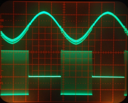
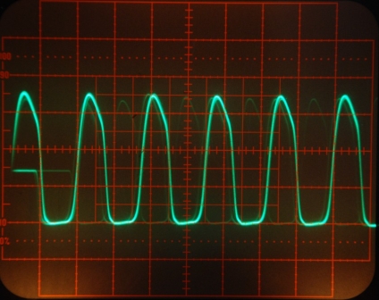
Top trace - TP-1
showing 6 KHz audio input signal.
The 3.1 MHz carrier is being
modulated at a 50% duty cycle by a 6000 Hz audio signal.
Note the very fast rise and fall times of the modulated RF
pulses.
This is the 100 watt peak power 3.1
MHz RF carrier output waveform as seen at the RF output
connector of the SSQ-2F ( TP3 ).
This is the 100 watt peak power 3.1
MHz RF carrier output waveform as seen at the RF output
connector of the SSQ-2F ( TP3 ).

This web site and all contents including pictures, text and diagrams is Copyright 2012 - 2026 by Ralph M Hartwell.
All Publication, Reproduction and Manufacturing Rights Reserved.